Journal of the Mexican Chemical Society, vol. 61, no. 4, 2017
Sociedad Química de México A.C.
F. Ambriz-Vargas *
INRS, Canada
R. Zamorano-Ulloa
Instituto Politécnico Nacional, Mexico
A. Romero-Serrano
Instituto Politécnico Nacional, Mexico
J. Ortiz-Landeros
Instituto Politécnico Nacional, Mexico
J. Crespo-Villegas
Instituto Politécnico Nacional, Mexico
D. Ramírez-Rosales
Instituto Politécnico Nacional, Mexico
C. Gómez-Yáñez
Instituto Politécnico Nacional, Mexico
Date received: 17 February 2017
Date accepted: 20 July 2017
Abstract: The present work shows the defect chemistry at room temperature of Bi4Ti3O12, emphasizing the effect of point defects on the ferroelectric properties. Electrical measurements of conductivity, dielectric permittivity and dielectric loss as well as structural characterization and Electron Spin Resonance (ESR) were used to deduce the existence of different point defects. Pure and Niobium doped bismuth titanate ceramic were prepared by a conventional solid state reaction technique. Rietveld refinement analysis suggested that niobium atoms occupy the titanium lattice sites and the presence of bismuth vacancies. Electron Spin Resonance measurements showed signals that are associated to iron impurities. The present communication supports the models of compensation mechanisms dominated by free electrons and bismuth vacancies.
Keywords: Ceramics, Dielectric properties, Point defects, Electrical properties.
Resumen: En el presente trabajo se estudia la química de defectos del Bi4Ti3O12 a temperatura ambiente, haciendo énfasis en el efecto de los defectos puntuales sobre las propiedades ferroelectricas. Mediciones de conductividad eléctrica, permitividad dieléctrica, perdida dieléctrica, caracterización estructural y resonancia de spin electrónico fueron utilizadas para demostrar la existencia de diferentes defectos puntuales. Titanato de Bismuto puro y dopado con niobio fueron sintetizados a partir del método convencional “Reacción del estado sólido”. El análisis de refinamiento de Rietveld reveló la formación de vacancias de bismuto al igual que la formación de átomos de niobio en los sitios atómicos del titanio, mientras que las mediciones de resonancia de spin electrónico revelaron señales asociadas a impurezas de hierro. El presente comunicado soporta mecanismos de compensación dominados por la presencia de electrones libres y vacancias de bismuto.
Palabras clave: Cerámicos, Propiedades dieléctricas, Defectos puntuales, Propiedades eléctricas.
1. Introduction
In recent years ferroelectric random access memories (FeRAMs) have attracted considerable attention to be applied as a nonvolatile technology, because they combine the DRAM benefits such as small cell size (22 F2, “F” stands for feature size), low voltage of operation and fast read/write access time (10ns/10ns), with nonvolatile data storage . One of the designs considers the use of a ferroelectric material in the capacitor of a FeRAM cell 5-7. Taking advantage of the polarization properties of the ferroelectric material, the positive and negative remnant polarization states could be codified as “0” and “1” digital states in a binary code 4, 8,9,10. However, the reading process requires a polarizing-depolarizing external action which implies fatigue problems 3, 7, 11. Bi4Ti3O12 has shown to be a good ferroelectric material for this application, the drawback of the pure compound is the relatively high leakage current. Lanthanum doping has shown to solve this problem 12.
The crystal structure of Bi4Ti3O12 can be described by titanium atoms surrounded by six oxygen atoms ([TiO6] clusters) in an octahedral configuration. These octahedrons are tilted into the orthorhombic structure. The [TiO6] clusters are sandwiched between the bismuth-oxide layers, while bismuth atoms are located in the corners of pseudo-perovskite units surrounding the [TiO6] octahedral clusters as shown in Fig. 1 13-14.
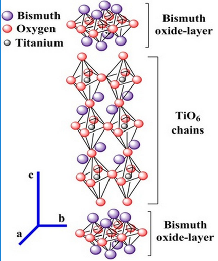
Fig. 1
Schematic representation of the crystal structure of Bi4Ti3O12.
The origin of the polarization properties in Bi4Ti3O12 is attributed to the tilting of the TiO6 octahedron cell from the c-axis and a-displacement of the bismuth atoms in the perovskite layer 15-16.
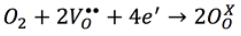
Recent studies have reported that the substitution of Ti4+ ions by Nb5+ ions in the crystal structure of Bi4Ti3O12, results in the improvement of the polarization properties 17-19. Since Nb5+ ions donate more electrons to the crystal structure than Ti4+ ions (Nb5+ ion is an aliovalent dopant), the electrical neutrality is disrupted, so spontaneous defect generation occurs to restore neutrality 20. Using the Kröger-Vink notation, the simplest compensations are:
 (1)
(1)
 (2)
(2)Titanium vacancies (V''' Bi ) could be included in Eq. (2) however, it is known that titanium vacancy formation requires a high amount of energy 21. Thus, it is possible that Nb doping compensation could be dominated by conduction electrons (e′) and bismuth vacancies (V''' Bi ).
Eqs. (1) and (2) suggest the simplest compensation mechanisms assuming that the only possible defects are holes (h ● ), free electrons (e′), Bismuth vacancies (V''' Bi ), Titanium vacancies (V'''' Ti ) and oxygen vacancies (Vö ). However it is clear, that the number of the different mechanisms of compensation depend not only on the concentration of Nb5+ ions but also on the presence of unavoidable impurities in the precursors and other possible defect complexes in the lattice 22-23.
The aim of this work is to contrast electrical properties, overall the polarization ones, with Eqs. (1) and (2) and to seek for other point defects using Electron Spin Resonance (ESR). To simplify variables the addition of lanthanum was deliberately avoided. It is well known that point defects have a strong influence on the polarization properties of a material, thus it is crucial to have a clear model about the defect chemistry of Bi4Ti3O12.
2. Materials and methods
Bi4Ti3O12 ceramic samples both pure and doped with Nb were fabricated by a conventional solid-phase reaction technique. TiO2 (Merck, 99% purity), Bi2O3 (Sigma-Aldrich, 99.9%) and Nb2O5 (Sigma-Aldrich, 99.9%) were used as starting reagents. All the powders were weighted and mixed in a polyethylene container with de-ionized water and zirconia balls (ZrO2). To homogenize the mixture, the container was rotated for 12 h and then heated in an oven at 80 °C for 18 h to remove moisture. Once dried, the powders were placed in a platinum crucible which was protected by an alumina plate inside of the furnace (Carbolite RHF 17/3E). The powder mixture was calcined at 1100°C (heating rate = 10 °C/min) in two steps. The first heating step was at 750°C during 2h to promote the formation of Bi4Ti3O12 and intermediate bismuth titanate phases. The second heating step was at 1100°C during 1h to obtain Bi4Ti3O12 single phase powders 24. In every step, the weight of the samples, before and after the thermal treatments was recorded in order to ensure that there was not a weight loss.
The solid solution formation can be written as:
 (3)
(3)From the above equation it can be observed that the oxidant character of the chamber (Pt crucible covered with alumina plate) increases when the dopant concentration increases.
The calcined powders were analyzed for the presence of phases using X-ray diffractometer (D8-focus Brucker diffractometer) equipped with Cu Kα radiation. Bi4Ti3O12 powders were uniaxially pressed into discs (115 MPa) and sintered in air at 1100 °C for 1 h 17. The lattice parameters and the unit cell volume were determined by the Rietveld method using the software “Topas-academic version 4.1” 25-26.
The above mentioned synthesis treatment was designed to accomplish the complete dissolution of the highest niobium concentration (2 at. %) into Bi4Ti3O12. Such determination was carried out by varying the dwell time of the furnace and measuring the lattice parameters. When the complete dissolution is accomplished the lattice parameters do not change anymore at longer dwell times. Moreover, sintered samples were mirror polished and the surface was observed through optical microscopy. Any secondary phase is commonly observed as small spots on the surface, but in this case, using the processing conditions described above only one phase was observed.
The microstructure analysis was carried by scanning electron microscopy (SEM, JEOL JSM-6701F) on polished and chemically etched surfaces. Based on literature, the chemical etching essays were carried out with HF/Nh4F/H2O (molar ratio 2:1.2:3, at 50ᵒC during 180 seconds) 27. The average grain size was determined using the micrographs and the linear intercept technique 24, 28.
To conduct the electrical characterization, Au-Pd electrodes were deposited by sputtering technique on each side of the discs. Copper wires were cold soldered onto the Au-Pd pads using silver paste. The entire device was covered with a high resistivity epoxy resin (Epolyglas MPT-M3, Mexico) 29. The room-temperature electrical conductivity, dielectric constant and dielectric loss factor were measured using LCR Meter Escort ELC-3133A at 1 kHz.
Hysteresis loops were recorded using an automatic Polarization-Electric field (P-E) loop tracer model RT-66A of Radiant Technologies brand 30-31.
Electron Spin Resonance (ESR) measurements of the ceramic powders were carried out at the X-band on a JEOL JES-RES 3X spectrometer, operating at 100 KHz field modulation. The ESR X-band spectra were recorded at 77K.
3. Results and discussion
3.1 Structural characterization
Fig. 2 (a) shows the X-ray diffraction patterns of the different solid solutions Bi4(Ti1-XNbX)3O12 (0.0<X<2 at. %). All patterns coincide with the XRD file for Bi4Ti3O12 (JCPDS file 035-0795). These results attest to the formation of pure Bi4Ti3O12 phase even when the niobium is introduced into Bi4Ti3O12 cell (There is not formation of any secondary phases related to unreacted precursors such as Nb2O3, TiO2 or BiO2). A zoom over the main characteristic planes of Bi4Ti3O12 is shown in Fig. 2 (b). In general, this figure shows displacements of the diffracted planes which indicates a solid solution formation and also it indicates a change in cell volume 25, 32-33.
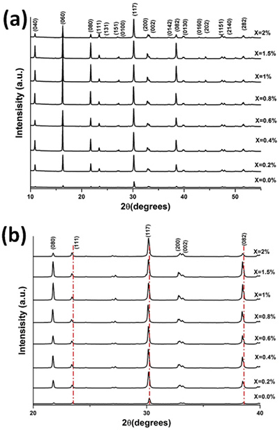
Fig. 2
X-ray patterns of the (a) Bi4(Ti1-X,NbX)3O12 solid solutions and (b) Zoom on the main characteristic peaks of Bi4Ti3O12
To understand the changes of Bi4Ti3O12 structural properties, a Rietveld analysis was performed in each sample to calculate the lattice parameters of the orthorhombic crystal structure of Bi4Ti3O12. Values of the quality factor (Rwp) were between 10.42 and 12.78 % which are in the range of the values reported for this material 26. As observed in Fig. 3, the lattice parameter “a”, “b” and “c” increased when the Nb concentration was increased. This behavior suggests that Nb5+ ions replaced the Ti4+ ions in the Bi4Ti3O12 crystal structure 25, it is well known that Nb5+ ions (78 pm) possess a slightly larger ionic radius than Ti4+ ions (74.5 pm) 25.
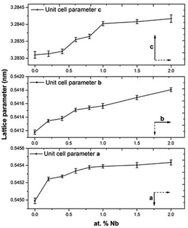
Fig. 3
Unit cell parameters a, b and c as a function of the Nb concentration.
As we expected, the volume of the unit cell of the solid solutions increased when the Nb5+ concentration was increased (Fig. 4). Different slopes are also observed in the behavior of each lattice parameters as a function of Nb content (Fig. 3) and hence, in the unit cell volume (Fig. 4), In fig. 4 m1 slope suggests the substitution of Ti4+ ions by Nb5+ ions, in the other hand m2 slope is related to the incorporation of Nb5+ ions into the Bi4Ti3O12 crystal structure as well as the formation of bismuth vacancies, these ones tend to reduce the growth rate of the unit cell volume.
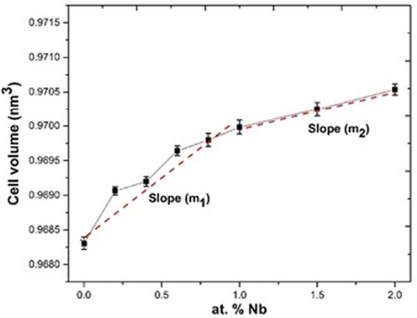
Fig. 4
Unit cell volume as a function of the Nb concentration.
3.2 Microstructural characterization
Fig. 5 shows the SEM micrograph of a chemical etched ceramic sample of Bi4Ti3O12 pellet. Generally, Plate-like grains are observed which are characteristic of this kind of materials and is a result of the strong anisotropy of the crystal structure 27, 34.
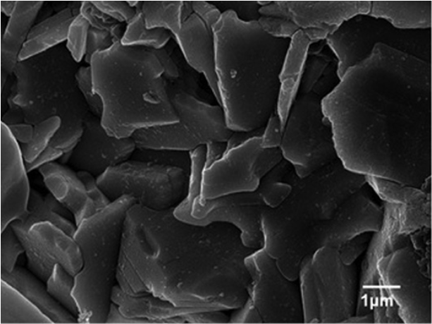
Fig. 5
SEM micrograph of Bi4Ti3O12 pellet.
The average grain size of the solid solutions decreases when the amount of niobium increases as it can be appreciated in Fig. 6. The average grain size decreases because the incorporation of niobium into the Bi4Ti3O12 distorts the crystalline lattice, hindering the propagation of the lattice through the space, hence, more grain boundaries will appear 29, 35.
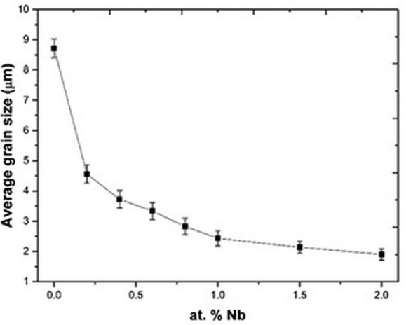
Fig. 6
Average grain size as a function of Nb concentration.
3.3 Electrical characterization
Electrical properties are shown in Figs. 7, 8 & 9. As observed, in these plots there are two different behaviors suggesting that these curves are closely related. At Nb concentrations smaller or equal to 0.8 atomic %, the conductivity increases when the Nb concentration increases (Fig.7). This increment in conductivity could be explained by the Eq. (1) where free electrons compensate the Nb substitution 17-20. Free electrons are polarizable entities so the dielectric permittivity increases in this range of Nb concentrations (Fig. 8), but due to these free electrons the polarization is rapidly lost by leakage, hence the dielectric loss also increases (Fig. 9) as a function of Nb concentration 29, 35.
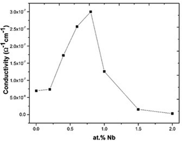
Fig. 7
Electrical conductivity of the Bi4(Ti1-X,NbX)3O12 solid solutions as a function of Nb concentration.
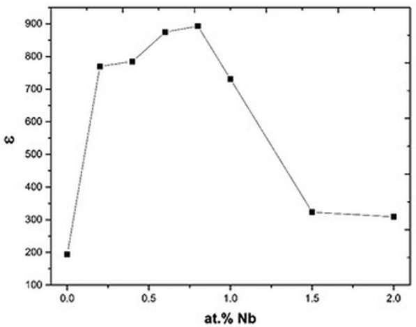
Fig. 8
Dielectric constant of the Bi4(Ti1-X,NbX)3O12 solid solutions, as a function of Nb concentration.
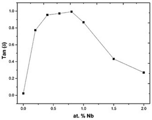
Fig. 9
Dielectric loss of the Bi4(Ti1-X,NbX)3O12 solid solutions as a function of Nb concentration.
At Nb concentrations greater than 0.8 atomic % the electrical conductivity decreases (Fig. 7), this supports Eq. (2) where bismuth vacancies become the main compensation mechanism. The decrement in the conductivity value is because this mechanism does not involve charge carriers 29, 35. In this range of dopant concentration, another resistivity source is the grain boundary as observed in Fig. 6. Then the low conductivity observed at Nb concentrations greater than 0.8 atomic % could be the result of the absence of charge carriers (Eq. 2) and the increment of the grain boundaries 36-37 (Fig. 6).
3.4 Polarization characterization
Fig. 10 shows the polarization loops for pure and 0.2 atomic % of niobium doped Bi4Ti3O12 ceramics. The loops do not show saturation 31, 38 and higher electric fields were not applied due to the risk of a breakdown. As observed in Fig. 10, there is a notorious increment in the loop area when the sample is doped which is commonly associated to a strong leakage current 39. In general this increment is related to dielectric loss 39-40. It can be seen in Figs. 11 and 12 that the loop area decreases when the dopant content increases which suggest that the dielectric loss value is strongly related to the hysteresis area.
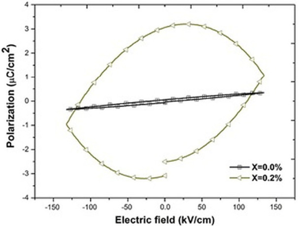
Fig. 10
Hysteresis loops of the Bi4(Ti1-X,NbX)3O12 solid solutions, with X, ranging from 0.0 to 0.2 at. %
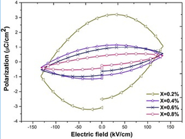
Fig. 11
Hysteresis loops of the Bi4(Ti1-X,NbX)3O12 solid solutions, with X, ranging from 0.2 to 0.8 at. %
However, the correspondence between the hysteresis areas (Figs. 10, 11 & 12) and the dielectric loss is not that perfect. According to Fig. 10 the biggest hysteresis area is presented for the 0.2 atomic % Nb sample but the highest loss is presented by the 0.8 atomic % Nb sample (Fig. 9). One source of dielectric loss is the presence of free electrons but another source is the presence of oxygen vacancies 41-42. It has been observed that oxygen vacancies have a domain pinning effect increasing the difficulty to polarize the material 17,18,19,20. As established in Eq. (3), when the dopant concentration is increased there is an increment of oxygen inside of the synthesis chamber or, in other words, the oxygen partial pressure is increased 43. Such dependence of the oxygen partial pressure on the dopant concentration is well described by Yet-Ming chang et all 44. This excess in oxygen could neutralize some oxygen vacancies in thermal equilibrium improving, hence, the ability of the material to respond to the external electric field 42, 45. The oxidation equation can be written as:
 (4)
(4)It is assumed that the oxidation process occurring during the synthesis (Eqs. 3 and 4), contributed to establish the oxygen vacancy concentrations in the samples at room temperature. In the present work the polarization at maximum electric field (either positive or negative) is named Pm. This value represents the ability of the material to be polarized at a given value of electrical field 46. Since the same range of electric field (in fact the same electric field pulse) was used in all samples to obtain the loops, it is possible to compare the ability to store electric charge among the samples. As observed in Figs. 10 and 11, for samples with Nb content smaller or equal to 0.8 atomic % there is not a clear trend in Pm values, however for samples with Nb content higher than 0.8 atomic % (Fig. 12) Pm decreases when the Nb content increases. It has been observed that both, oxygen and bismuth vacancies are detrimental of the polarization properties 17,18,19,20, 31, 47. It is well known that the main structural cause of polarization in Bi4Ti3O12 is the a-axis displacement of bismuth atoms in the perovskite site 42, 45. In the range of 0-0.2 Nb atomic %, oxygen vacancies are annihilated by the oxidizing atmosphere 42-43, as it was mentioned before; hence Pm value increases when 0.2 atomic % of Nb is incorporated in the crystal lattice (Fig. 10). At higher Nb concentration there is also a depolarizing effect due to free electrons (Eq. 1 and Fig. 7) so Pm decreases between 0.2 and 0.8 Nb atomic % 42.
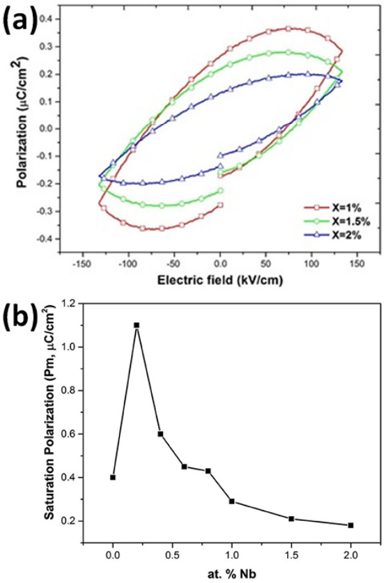
Fig. 12
(a) Hysteresis loops of the Bi4(Ti1-X,NbX)3O12 solid solutions, with X, ranging from 1 to 2 at. % and (b) Summary of the “Polarization vs electric field” results (Saturation polarization as a function of Nb dopant content)
At Nb concentrations higher than 0.8 atomic % the compensation mechanism (2) dominates, therefore there is an increment in the bismuth vacancies concentration leading to a decrement of Pm value (Fig.12(a)) 45. A summary of effect of niobium on the polarization properties of Bi4Ti3O12 is shown in Fig. 12 (b).
3.5 ESR analysis of Bi 4 Ti 3 O 12
Fig. 13 shows the ESR spectra of the undoped Bi4Ti3O12. This ESR spectrum shows well-defined signals labeled A, B and C
In sake to avoid confusion and to be consistent to the Kröger-Vink notation, the complex defect for the A signal could be written as.
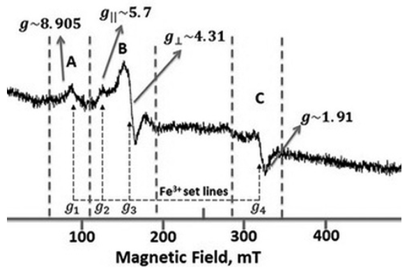
Fig. 13
ESR spectrum of Bi4Ti3O12 at 77 K and microwave frequency of 9.1489 GHz.
A signal
Iron (Fe) is a common impurity in precursors and it is reported by the manufacturer a concentration of around 0.005% in TiO2 hence it can be considered that A and B defects are marginal in the material.
As one can see the main part of the Fe3+ set lines contribute to a complex superposition of the ESR signals (𝑔1~8.905, 𝑔2~5.7, 𝑔3~4.31 𝑎𝑛d 𝑔4~2.05) 52. In other words, the ESR Fe3+ signal has to do with the A, B and C signals.
The wide A signal with 𝑔~8.905 was assigned to Fe3+ ions located in Ti4+ sites where oxygen octahedral have lost an oxygen atom to compensate charge and so leading to a strong crystal distortion 34. There are several reports related to A signal, where it was observed at around 73.4 mT (like in Fig. 13) in BaTiO353. All of these reports associate the signal to a defect with g(9. However, it is not clear whether the oxygen vacancy is neutral or not. Some reports suggest that the entire defect acts as an electron deep trap 54-55. If the vacancies were associated with two positive charges, this defect would produce the B signal so the electrical charge associated with the oxygen vacancy remains unclear. All the reports agree that this ESR signal comes from the Fe3+ ion which is substituting the Ti4+ ion in the lattice 55.
In the present work the A signal corresponds to the center (Fe′𝑇𝑖 - 𝑉𝑂)′ with 𝑔~8.905.
B signal
When the Fe3+ ion substitutes the Ti4+ ion, a negative charge center at Fe site will be created (Fe′𝑇𝑖). In that case, the negative center could attract an oxygen vacancy (Vö) around it producing a single charged F+ center 49.
The B signal represents two resonances, the first resonance at H~124.26𝓂T is representative for the center (Fe′𝑇𝑖 - Vö) ( ‖ with 𝑔‖~5.7, while the second resonance at 𝐻~157.6 𝑚𝑇 is due to a center (Fe′𝑇𝑖 - Vö)( ⊥ with 𝑔⊥~4.31.
C signal
The C signal in Fig. 13 most likely belongs to the center (𝑇𝑖′𝑇𝑖-Vö) ( at H~340𝓂T and 𝑔~1.91 50-51 although there is some influence of the Fe3+ ions.
The change in oxidation state from Ti4+ to Ti3+ is commonly observed in reducing atmospheres 50-51. At normal pressure this reduction occurs at high temperatures. Hence, these defects could be produced during the synthesis of Bi4Ti3O12 powders. As a defect equation, this reaction can be written as:
 (5)
(5)The material can compensate this substitution in different ways but to produce the C signal (Fig. 13) some reports suggest the presence of a oxygen vacancy giving a complex defect with a net positive charge (F+ center) 50-51, 54. Since the synthesis conditions were carry out in a oxidative atmosphere (Eq. 3) it is expected a marginal Ti3+ concentration and therefore, small influence of (𝑇𝑖′𝑇𝑖-Vo (( )( complex on the properties.
3.6 ESR analysis of Nb doped Bi 4 Ti 3 O 12
The effect of Nb doping on the ESR graphs is shown in Figs. 14 and 15. When the Nb concentration increases, the intensities of A and C signals decrease (Figs. 14 and 15) in all the concentrations studied in this work. However, regarding the B signal there are two cases: for Nb concentrations smaller or equal to 0.8 atomic %, when the Nb concentration increases the intensity of the B signal decreases (Fig. 14), whereas for concentrations higher than 0.8 atomic % (Fig. 15) the contrary occurs.
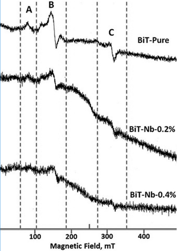
Fig. 14
ESR spectrum of the Bi4(Ti1-X,NbX)3O12 solid solutions with X, ranging from 0.0 to 0.4 at. %, at 77 K and microwave frequency of 9.1489 GHz.
The behavior of the A and C signal intensities with respect to Nb concentration could be explained by the oxidation associated with the doping process (Eqs. 3 and 4). Oxidation could explain the reduction of 𝑉𝑂 and Ti3+ populations 42 (Figs. 14 and 15), but in the case of B signal, its behavior seems to correspond to the compensation mechanisms (Eqs. 1 and 2) very well; at low Nb concentrations (Fig. 14), the B signal disappears, suggesting a relationship with the free electrons present at these concentrations (Fig. 7). At higher Nb concentrations (Fig. 15), the B signal does not disappear, that might be due to the absence of free electrons. This signal survives, though, the oxidative conditions at high Nb concentrations. Hence, the results suggest that the signal B is deactivated in the ESR graph, by the presence of free electrons 22-23.
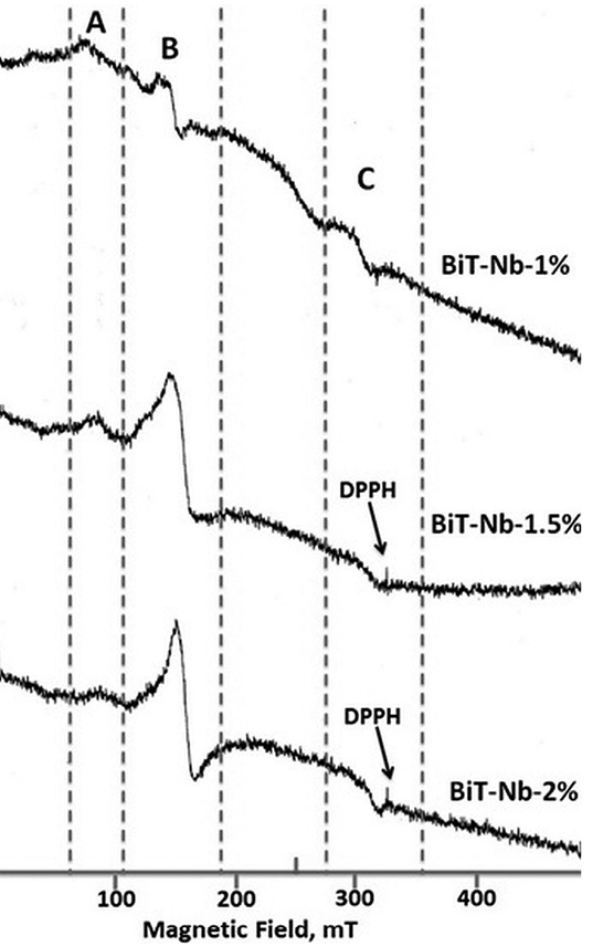
Fig. 15
ESR spectrum of the Bi4(Ti1-X,NbX)3O12 solid solutions with X, ranging from 1 to 2 at. %, DPPH is the standard sample with g = 2.
4. Conclusions
Values of conductivity, dielectric permittivity, dielectric loss, and lattice parameters as function of Nb additions into the Bi4Ti3O12 crystal lattice coincide very well with the existence of two compensation mechanisms used by the material to re-establish electrical neutrality, namely, free electrons and bismuth vacancies. Compensation by free electrons seems to dominate at Nb concentrations lower than 0.8 atomic %, whereas at higher Nb concentrations, bismuth vacancies seem to be the dominant compensation mechanism.
The characteristics of hysteresis P-E loops seem to depend only on the presence of free electrons, oxygen vacancies and bismuth vacancies.
ESR analysis revealed the defect complexes, (and centers in the Bi4Ti3O12 sample. ESR results suggest that the first and third ESR signals were neutralized by an oxidation process whereas the ESR signal of the second defect seems to depend on the existence of free electrons. Since the presence of Fe in this case is marginal, it is considered that the Fe associated defects have a minor influence on the electric properties. On the other hand, the concentration of Ti3+ is also marginal because the material was processed in oxidizing conditions during this work, where the ion tends to change its oxidation state to Ti4+.
Acknowledgements
Financial support from Fonds de Recherché du Quebec-Nature et Technologies (FRQNT); The Natural Sciences and Engineering Research Council of Canada (NSERC) and the National Science and Technology Council of Mexico (CONACyT) is gratefully acknowledged.
References
1. 1. Mikolajick, T.; Dehm, C.; Hartner, W.; Kasko, I.; Kastner, M.J.; Nagel, N.; Moert, M.; Mazure, C.; Microelectronics Reliability 2001, 41, 947-950.
2. 2. Baldi, L.; Bez, R.; Sandhu, G. Solid-State Electronics 2014, 102, 2-11.
3. 3. Fabian, A.; Gitanjali, K.; Maxime, B.; Azza H.; Rafik N.; Andranik, S.; Reji, T.; Carlos G. Marc, A. G.; Andreas, R. ACS Appl. Mater. Interfaces 2017, 9 (15), 13262-13268.
4. 4. Jeong, D. S.; Thomas, R.; Katiyar, R. S.; Scott, J. F.; Kohlstedt, H.; Petraru, A.; Hwang, C. S. Rep Prog Phys 2012, 75 (7), 076502.
5. 5. Kao, M. C.; Chen, H. Z.; Young, S. L.; Chuang, B. N.; Jiang, W. W.; Song, J. S.; Jhan, S. S.; Chiang, J. L.; Wu, L. T. J. Cryst. Growth 2012, 338 (1), 139-142.
6. 6. Kohlstedt, H.; Mustafa, Y.; Gerber, A.; Petraru, A.; Fitsilis, M.; Meyer, R.; Böttger, U.; Waser, R. Microelectron. Eng. 2005, 80, 296-304.
7. 7. Fabian, A.; Ivan, V.; Thomas, R.; Ruediger, A. J. Vac. Sci. Technol., B: Nanotechnol. Microelectron.: Mater., Process., Meas., Phenom. 2016, 34 (2), 02M101.
8. 8. Kang, S. W. R. J. Mater. Sci.: Mater. Electron. 2004, 2004, 231-234.
9. 9. Makarov, A.; Sverdlov, V.; Selberherr, S. Microelectron. Reliab. 2012, 52 (4), 628-634.
10. 10. Fabian, A.; Gintanjali, K.; Thomas, R.; Nouar, R.; A. Sarkissian, Carlos, G.; Marc, G.; Ruediger, A. Appl. Phys. Lett. 2017, 110, 093106
11. 11. Soni, R.; Petraru, A.; Meuffels, P.; Vavra, O.; Ziegler, M.; Kim, S. K.; Jeong, D. S.; Pertsev, N. A.; Kohlstedt, H. Nat Commun 2014, 5, 5414.
12. 12. Wu, A.; Soares, M. R.; Miranda Salvado, I. M.; Vilarinho, P. M. Mater. Res. Bull. 2012, 47 (11), 3819-3824.
13. 13. Oliveira, R. C.; Cavalcante, L. S.; Sczancoski, J. C.; Aguiar, E. C.; Espinosa, J. W. M.; Varela, J. A.; Pizani, P. S.; Longo, E. J. Alloys Compd. 2009, 478 (1-2), 661-670.
14. 14. Martin, L. W.; Chu, Y. H.; Ramesh, R. Mater. Sci. Eng. 2010, 68 (4-6), 89-133.
15. 15. Noguchi, T. G.; Miyayama, M.; Hoshikawa, A.; Kamiyama, T. J Electroceram 2008, 21, 49-54.
16. 16. Materlik, R.; Künneth, C.; Kersch, A. J. Appl. Phys. 2015, 117 (13), 134109.
17. 17. Zhang, L.; Chu, R.; Zhao, S.; Li, G.; Yin, Q. Mater. Sci. Eng: B 2005, 116 (1), 99-103.
18. 18. Bao, Z.H.; Zhu, J.S.; Wang, J.S. Mater. Lett. 2002, 56, 861- 866.
19. 19. Lee, S.-Y.; Park, B.-O. J. Cryst. Growth 2005, 283 (1-2), 81-86.
20. 20. Simões, A. Z.; Aguiar, E. C.; Ries, A.; Longo, E.; Varela, J. A. Mater. Lett. 2007, 61 (2), 588-591.
21. 21. Nowotny, M. K.; Nowotny, J. J. Phys. Chem. B 2006, 110, 16283-16291.
22. 22. Laguta, V. V.; Slipenyuk, A. M.; Bykov, I. P.; Glinchuk, M. D.; Maglione, M.; Michau, D.; Rosa, J.; Jastrabik, L. Appl. Phys. Lett. 2005, 87 (2), 022903.
23. 23. Laguta, V. V.; Slipenyuk, A. M.; Bykov, I. P.; Glinchuk, M. D.; Maglione, M.; Bilous, A. G.; V′yunov, O. I.; Rosa, J.; Jastrabik, L. J. Appl. Phys. 2005, 97 (7), 073707.
24. 24. Santos, J. C.; Mir, M.; Mastelaro, V.R.; Hernandes, A.C. J. Eur. Ceram. Soc. 2009, 751-756.
25. 25. Jose, O.; Carlos, G. ; Palacios-Romero, C.; Lima, E.; Pfeiffer, H. J Phys Chem A 2012, 116 (12), 3163-71.
26. 26. Machura, D.; Rymarczyk, J.; Ilczuk, J. Eur. Phys. J.: Spec. Top. 2008, 154 (1), 131-134.
27. 27. Jardiel, T.; Caballero, A. C.; Fernández, J. F.; Villegas, M. J. Eur. Ceram. Soc. 2006, 26 (13), 2823-2826.
28. 28. Kim, H. J.; Park, M. H.; Kim, Y. J.; Lee, Y. H.; Jeon, W.; Gwon, T.; Moon, T.; Kim, K. D.; Hwang, C. S. Appl. Phys. Lett. 2014, 105 (19), 192903.
29. 29. Paredes-Olguín, M.; Lira-Hernández, I. A.; Gómez-Yáñez, C.; Espino-Cortés, F. P. Phys. B 2013, 410, 157-161.
30. 30. Tao, L. L.; Wang, J. J. Appl. Phys. 2016, 119 (22), 224104.
31. 31. Park, M. H.; Lee, Y. H.; Kim, H. J.; Kim, Y. J.; Moon, T.; Kim, K. D.; Muller, J.; Kersch, A.; Schroeder, U.; Mikolajick, T.; Hwang, C. S. Adv Mater 2015, 27 (11), 1811-31.
32. 32. Velasco-Davalos, I.; Ambriz-Vargas, F.; Gómez-Yáñez, C.; Thomas, R. ; Ruediger, A. J. Alloys Compd. 2016, 667, 268-274.
33. 33. Velasco-Davalos, I. ; Ambriz-Vargas, F. ; Kolhatkar, G.; Thomas, R. ; Ruediger, A. AIP Advances 2016, 6 (6), 065117.
34. 34. Velasco-Davalos, I. A.; Moretti, M.; Nicklaus, M.; Nauenheim, C.; Li, S.; Nechache, R.; Gomez-Yanez, C.; Ruediger, A. Appl. Phys. A: Mater. Sci. Process. 2013, 115 (3), 1081-1085.
35. 35. Velasco-Davalos, I. A.; Ruediger, A. ; Cruz-Rivera, J. J.; Gomez-Yanez, C. J. Alloys Compd. 2013, 581, 56-58.
36. 36. Yoo, Y. W.; Jeon, W.; Lee, W.; An, C. H.; Kim, S. K.; Hwang, C. S. ACS Appl Mater Interfaces 2014, 6 (24), 22474-82.
37. 37. Plutenko, T. A.; V′yunov, O. I.; Belous, A. G. Inorg. Mater. 2012, 48 (12), 1183-1189.
38. 38. Chen, M.; Liu, Z. L.; Wang, Y.; Wang, C. C.; Yang, X. S.; Yao, K. L. Phys. B 2004, 352 (1-4), 61-65.
39. 39. Chen, X. Q.; Yang, F. J.; Cao, W. Q.; Wang, H.; Yang, C. P.; Wang, D. Y.; Chen, K. Solid State Commun. 2010, 150 (27-28), 1221-1224.
40. 40. Cheng, Z. X.; Li, A. H.; Wang, X. L.; Dou, S. X.; Ozawa, K.; Kimura, H.; Zhang, S. J.; Shrout, T. R. J. Appl. Phys. 2008, 103 (7), 07E507.
41. 41. Shimizu, T.; Yokouchi, T.; Oikawa, T.; Shiraishi, T.; Kiguchi, T.; Akama, A.; Konno, T. J.; Gruverman, A.; Funakubo, H. Appl. Phys. Lett. 2015, 106 (11), 112904.
42. 42. Noguchi, Y.; Yamamoto, K.; Kitanaka, Y.; Miyayama, M. J. Eur. Ceram. Soc. 2007, 27 (13-15), 4081-4084.
43. 43. Kolodiazhnyi, T. J. Phys. chem. Solids 2003, 64, 953-960.
44. 44. Chang, Y.; Kingery, W. D. Defects in Ceramics, J. Wiley 1997, 129-130.
45. 45. Noguchi, Y.; Goto, T.; Miyayama, M.; Hoshikawa, A.; Kamiyama, T. J. Electroceram. 2007, 21 (1-4), 49-54.
46. 46. Chen, M.; Huang, K.-l.; Mei, X.-a.; Huang, C.-q.; Liu, J.; Cai, A.-h. Trans. Nonferrous Met. Soc. China 2009, 19 (1), 138-142.
47. 47. Chiu, H.-C.; Wu, C.-H.; Chi, J.-F.; Chien, F.-T. Microelectron. Reliab. 2014, 54 (6-7), 1282-1287.
48. 48. Murugaraj, P. J. Mater. Sci. Lett 1986, 5, 171-173.
49. 49. Jakes, P.; Erdem, E.; Eichel, R.-A.; Jin, L.; Damjanovic, D. Appl. Phys. Lett. 2011, 98 (7), 072907.
50. 50. Zhang, Z. H.; Wu, S. Y.; Kuang, M. Q.; Song, B. T. Eur. Phys. J.: Appl. Phys. 2011, 56 (1), 10303.
51. 51. Eichel, R. A. Phys Chem Chem Phys 2011, 13 (2), 368-84.
52. 52. Shelef, A. J. Catal. 2000, 195, 106-112.
53. 53. Issa, M. A.; Dughaish, Z. H. J. Phys. D: Apple. Phys 1984, 17, 2037-2047.
54. 54. Glinchuk, M. D.; Kornienko, S. M.; Laguta, V. V.; Slipenyuk, A. M.; Bilous, A. G.; V′yunov, O. I.; Yanchevskii, O. Z. J. Mater. Chem. 2000, 10, 941-947.
55. 55. Kornienko, M.; Glinchuk, M. D.; Laguta, V.V.; Belous, A. G.; Yastrabik, L. Phys. Solid State 1999, 41, 1838-1842.
Author notes
*Corresponding Author: *Phone: +1.514.228.6978 E-mail: fabian.ambriz.vargas@emt.inrs.ca Postal address: 1650, Boulevard Lionel Boulet, Varennes, Québec, J3X 1S2, CANADA.
